13761090949

當前位置:首頁 > 產(chǎn)品中心 > 二維材料 > 碲化物晶體 > GaTe 碲化鎵晶體 (Gallium Telluride)


簡要描述:Our single crystal monoclinic GaTe (Gallium telluride) crystals come with guaranteed anisotropy, electronic, and optical grade crystal quality.
 產(chǎn)品型號: 廠商性質(zhì):生產(chǎn)廠家更新時間:2024-06-04訪 問 量:1376
相關文章
Related Articles詳細介紹
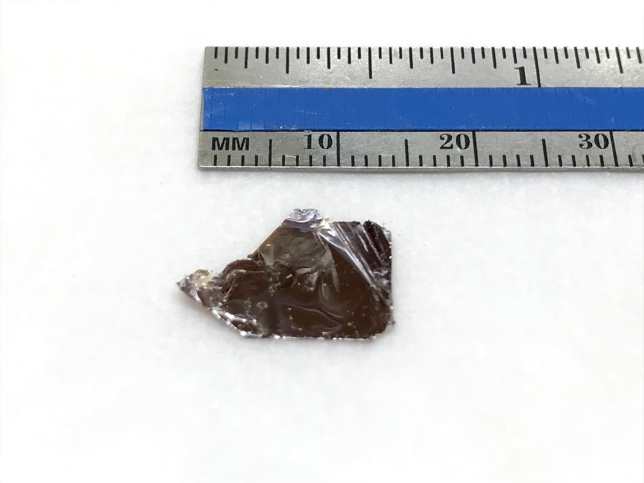
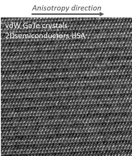
Our single crystal monoclinic GaTe (Gallium telluride) crystals come with guaranteed anisotropy, electronic, and optical grade crystal quality. They are developed at our facilities using three different growth techniques, namely Bridgman growth, chemical vapor transport (CVT), and flux zone growth, to optimize grain sizes and reduce defect concentrations. In contrast to commonly used chemical vapor transport (CVT) technique, flux grown crystals are well known for their structural perfection and electronic/optical performance. Bridgman and flux zone methods both offer similar grade qualities. Each crystal very large in size to last for years, is highly crystalline, oriented in 0001 direction, and easy to exfoliate. Our R&D staff takes characterization dataset in each sample piece to ensure structural, optical, and electronic consistency.
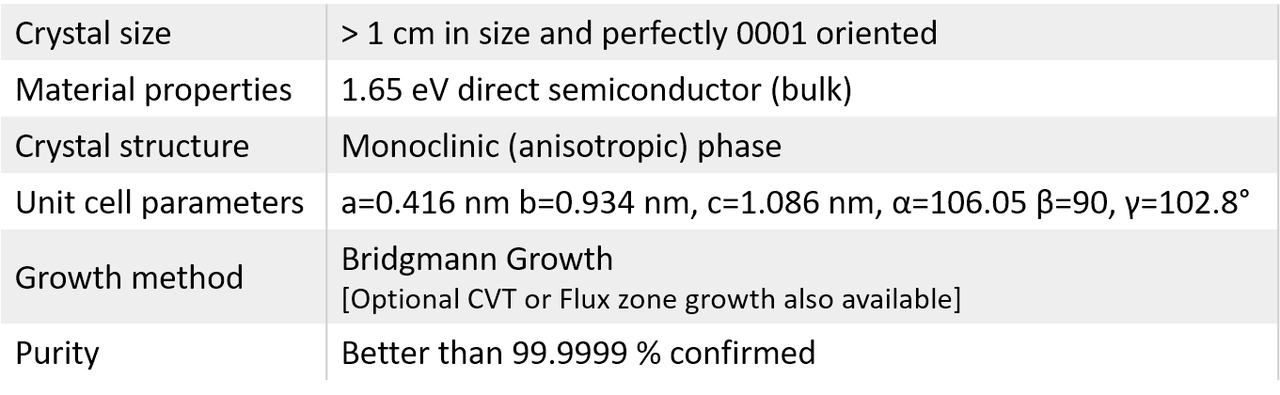
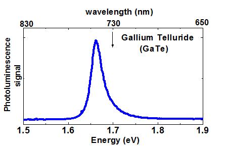
Properties of monoclinic GaTe vdW crystals
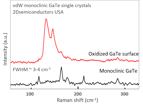
Growth method matters> Flux zone or CVT growth method? Contamination of halides and point defects in layered crystals are well known cause for their reduced electronic mobility, reduced anisotropic response, poor e-h recombination, low-PL emission, and lower optical absorption. Flux zone technique is a halide free technique used for synthesizing truly semiconductor grade vdW crystals. This method distinguishes itself from chemical vapor transport (CVT) technique in the following regard: CVT is a quick (~2 weeks) growth method but exhibits poor crystalline quality and the defect concentration reaches to 1E11 to 1E12 cm-2 range. In contrast, flux method takes long (~3 months) growth time, but ensures slow crystallization for perfect atomic structuring, and impurity free crystal growth with defect concentration as low as 1E9 - 1E10 cm-2. During check out just state which type of growth process is preferred. Unless otherwise stated, 2Dsemiconductors ships Flux zone crystals as a default choice.
產(chǎn)品咨詢
聯(lián)系我們
上海巨納科技有限公司 公司地址:上海市虹口區(qū)寶山路778號海倫國際大廈5樓 技術支持:化工儀器網(wǎng)掃一掃 更多精彩

微信二維碼

網(wǎng)站二維碼
 歡迎來到
歡迎來到