 歡迎來(lái)到上海巨納科技有限公司網(wǎng)站!歡迎來(lái)到上海巨納科技有限公司網(wǎng)站!
13761090949

當(dāng)前位置:首頁(yè) > 產(chǎn)品中心 > 二維材料 > 硒化物晶體 > PtSe2 二硒化鉑晶體 (Platinum Diselenide)


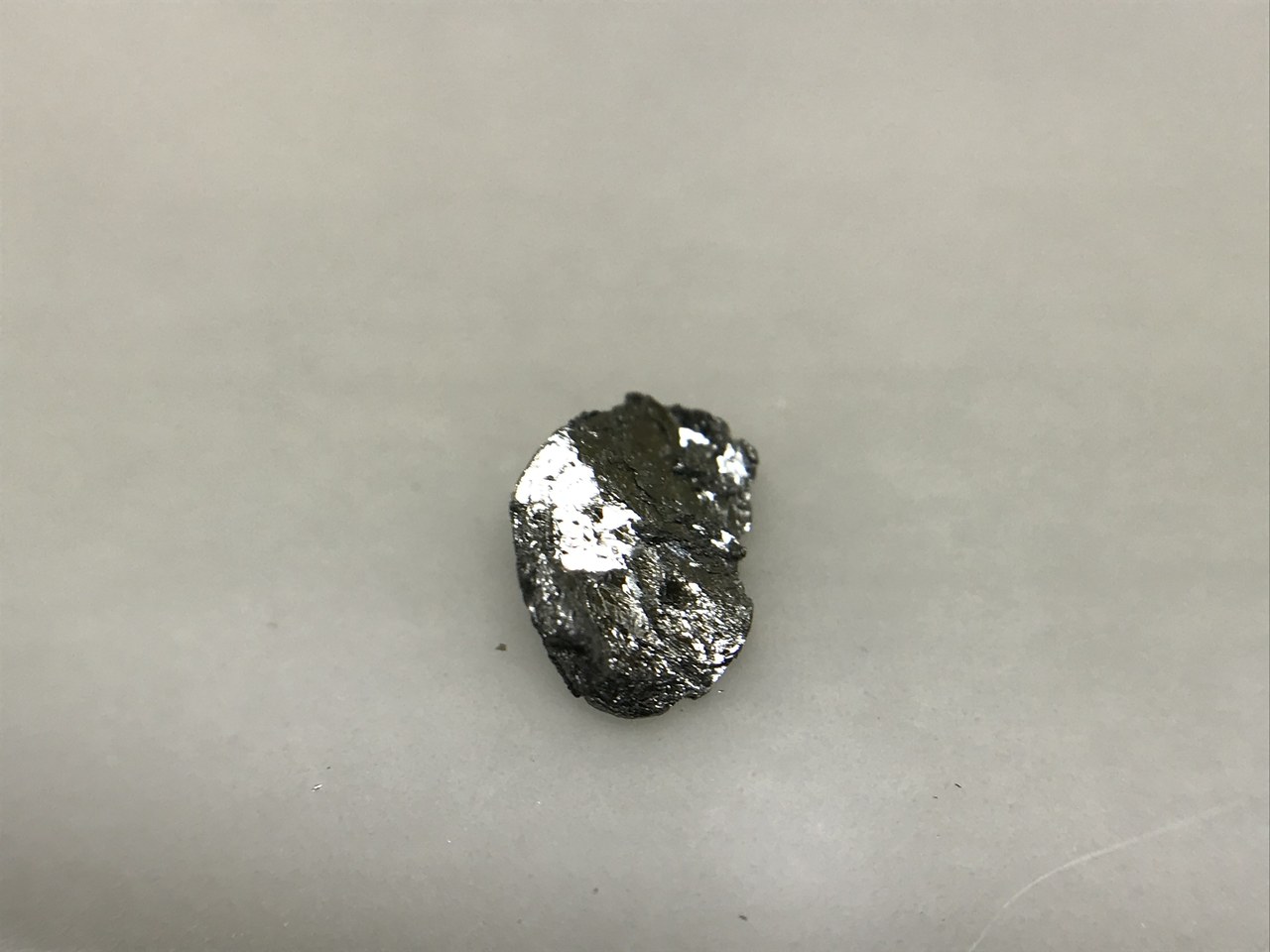
簡(jiǎn)要描述:Platinum diselenide (PtSe2) is a member of transition metal dichalcogenide (TMDCs) family with the MX2 formula.
 產(chǎn)品型號(hào): 廠商性質(zhì):生產(chǎn)廠家更新時(shí)間:2024-06-03訪 問(wèn) 量:1387
相關(guān)文章
Related Articles詳細(xì)介紹
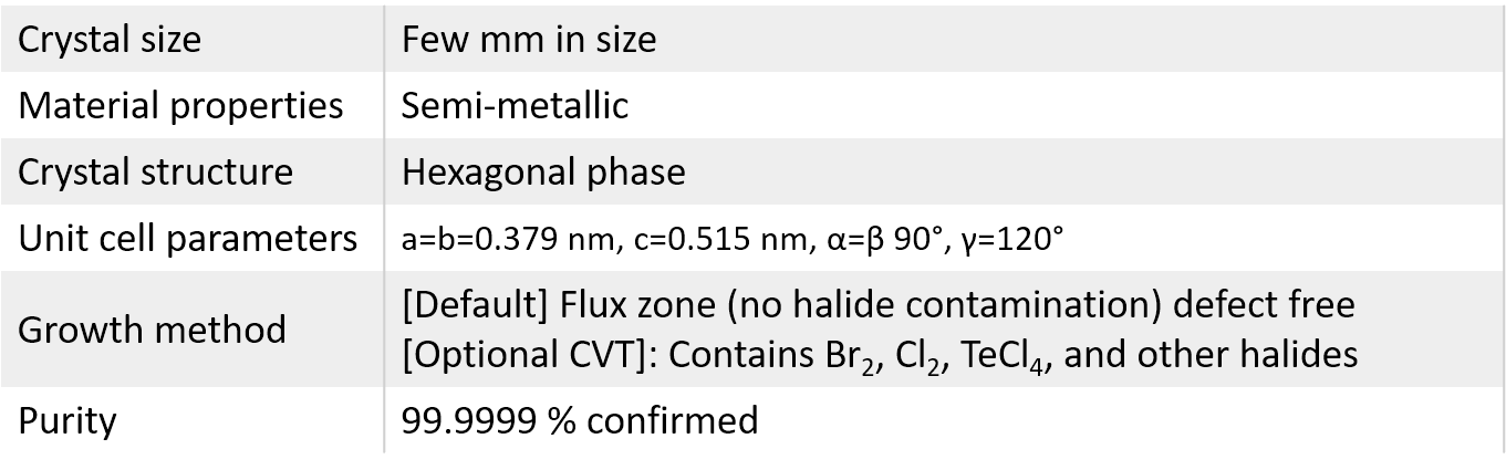
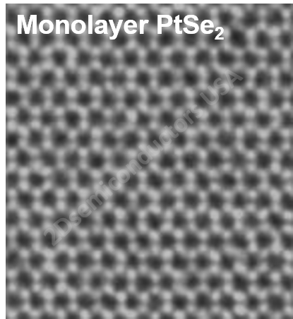
Platinum diselenide (PtSe2) is a member of transition metal dichalcogenide (TMDCs) family with the MX2 formula. While it is an established semimetal in the bulk form the band gap of its monolayer has been recently predicted to be a semiconductor (Nano Letters, 2015, 15, 4013).
Growth method matters> Flux zone or CVT growth method? Contamination of halides and point defects in layered crystals are well known cause for their reduced electronic mobility, poor e-h recombination, low-PL emission, and lower optical absorption. Flux zone technique is a halide free technique used for synthesizing truly semiconductor grade vdW crystals. This method distinguishes itself from chemical vapor transport (CVT) technique in the following regard: CVT is a quick (~2 weeks) growth method but exhibits poor crystalline quality and the defect concentration reaches to 1E11 to 1E12 cm-2 range. In contrast, flux method takes long (~3 months) growth time, but ensures slow crystallization for perfect atomic structuring, and impurity free crystal growth with defect concentration as low as 1E9 - 1E10 cm-2. So if your research needs truly high quality crystals for optoelectronics, scanning tunneling microscopy, spectroscopy, and other projects that rely on defect free crystals, flux zone growth is ideal for you. However, if you need catalytic materials presence of defects typically helps and in such case CVT method is better suited. During check out just state which type of growth process is preferred. Unless otherwise stated, 2Dsemiconductors ships Flux zone crystals as a default choice.
Properties of PtSe2 crystals by 2Dsemiconductors USA
產(chǎn)品咨詢
聯(lián)系我們
上海巨納科技有限公司 公司地址:上海市虹口區(qū)寶山路778號(hào)海倫國(guó)際大廈5樓 技術(shù)支持:化工儀器網(wǎng)掃一掃 更多精彩

微信二維碼

網(wǎng)站二維碼