13761090949

當(dāng)前位置:首頁 > 產(chǎn)品中心 > 二維材料 > 硒化物晶體 > ReSe2 二硒化錸晶體 (Rhenium Diselenide)


簡要描述:Single crystal ReSe? (Rhenium diselenide) crystals are developed at our facilities using chemical vapor transport or flux zone technique methods after 8 years of growth optimization to ensure anisotro
 產(chǎn)品型號: 廠商性質(zhì):生產(chǎn)廠家更新時(shí)間:2024-06-03訪 問 量:1191
相關(guān)文章
Related Articles詳細(xì)介紹
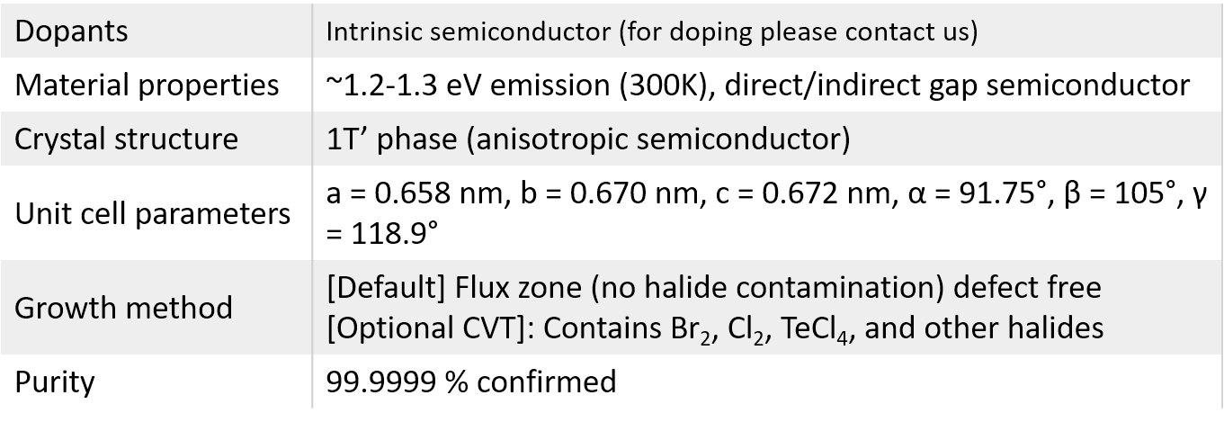
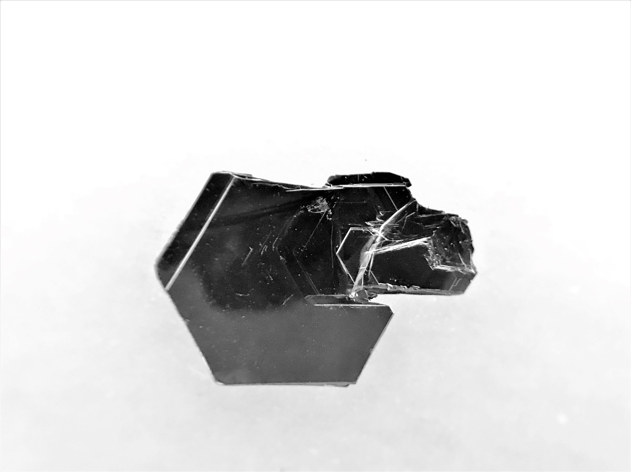
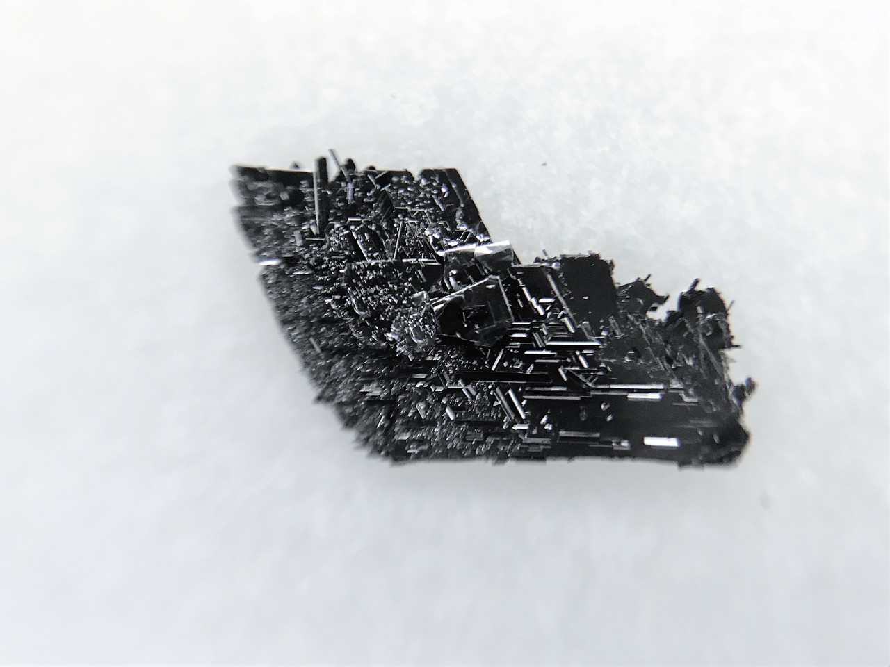
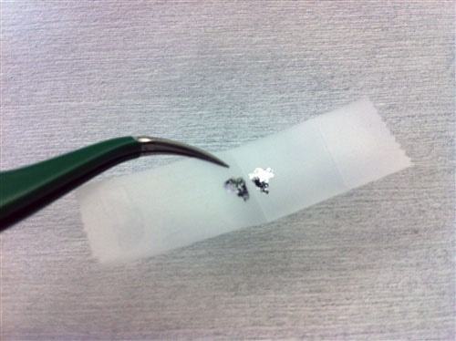
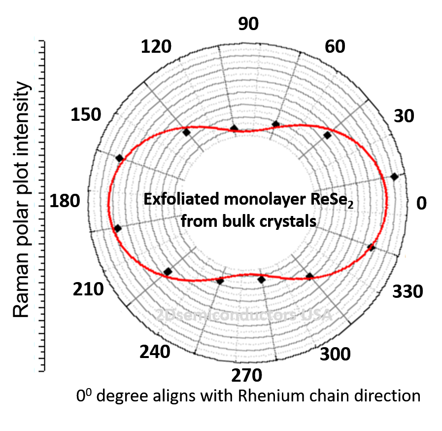
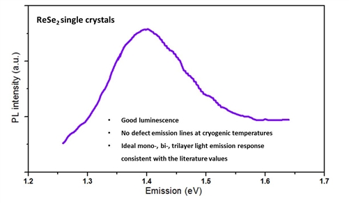
Single crystal ReSe? (Rhenium diselenide) crystals are developed at our facilities using chemical vapor transport or flux zone technique methods after 8 years of growth optimization to ensure anisotropic properties. Our ReSe2 crystals display impressive structural anisotropy from bulk down to monolayers as evidenced by TEM and angle resolved Raman spectroscopy measurements (see XRD, TEM, Raman, PL, and other figures below). Our ReSe2 crystals that guarantees crystalline, optical, and electronic anisotropy at large scales. Crystals are rather large in size, perfectly layered, and ready for exfoliation. Our R&D team also provides you with transfer technique to boost your monolayer yield rate up to 95%. If your research needs doped ReSe2 crystals, we can introduce Mo, Au, Nb, and other dopants.
Typical characteristics of ReSe2 crystals from 2Dsemiconductors
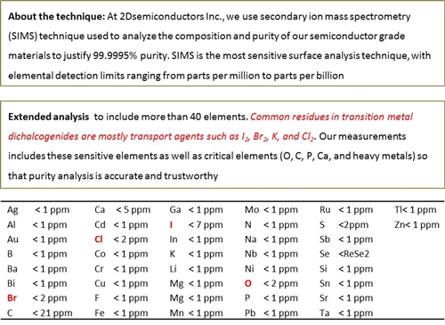
Growth method matters> Flux zone or CVT growth method? Contamination of halides and point defects in layered crystals are well known cause for their reduced electronic mobility, reduced anisotropic response, poor e-h recombination, low-PL emission, and lower optical absorption. Flux zone technique is a halide free technique used for synthesizing truly semiconductor grade vdW crystals. This method distinguishes itself from chemical vapor transport (CVT) technique in the following regard: CVT is a quick (~2 weeks) growth method but exhibits poor crystalline quality and the defect concentration reaches to 1E11 to 1E12 cm-2 range. In contrast, flux method takes long (~3 months) growth time, but ensures slow crystallization for perfect atomic structuring, and impurity free crystal growth with defect concentration as low as 1E9 - 1E10 cm-2. During check out just state which type of growth process is preferred. Unless otherwise stated, 2Dsemiconductors ships Flux zone crystals as a default choice.
產(chǎn)品咨詢
聯(lián)系我們
上海巨納科技有限公司 公司地址:上海市虹口區(qū)寶山路778號海倫國際大廈5樓 技術(shù)支持:化工儀器網(wǎng)掃一掃 更多精彩

微信二維碼

網(wǎng)站二維碼
 歡迎來到
歡迎來到